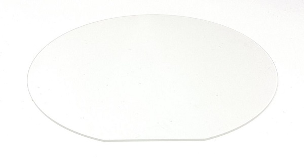
Glass and Fused Silica Wafers
Glass and Fused Silica Wafers
Description

Glass and fused silica wafers are both commonly used in the semiconductor industry, but they have different properties and applications.
Glass wafers are typically made from various types of glass, including soda-lime, borosilicate, and quartz. They are often used in applications where optical clarity is not critical, such as for MEMS devices, sensors, and microfluidics. Glass wafers can be easily mass-produced, making them ideal for high-volume manufacturing processes, and they are typically less expensive than fused silica wafers.
Fused silica wafers, on the other hand, are made from a high-purity glass made from silicon dioxide that has been melted and then rapidly cooled to form a solid. Fused silica wafers are often used in applications where optical clarity and dimensional stability are critical, such as for optical components like lenses, prisms, and mirrors. Fused silica wafers have excellent optical properties, including high transparency and low birefringence, as well as high resistance to thermal and chemical damage. They are also dimensionally stable, meaning that they maintain their shape and size even when exposed to changes in temperature or humidity.
In summary, while glass wafers are often less expensive and suitable for applications where optical clarity is not critical, fused silica wafers are preferred for applications requiring high-quality optical properties and dimensional stability.
We offer glass wafers of the following types:
| BK7 substrates | Quartz microscope slides | Fused Silica | Selected float glass substrates |
| BOROFLOAT® substrates | MEMpax® substrates | B270 Superwite substrates | 1737F substrates |
| EAGLE2000 substrates | 7059 substrates | D 263T substrates | AF 32 eco substrates |
| AS87 eco substrates | Borosilicate glass substrates | Infrared blocking substrates | Partially transmitting substrates |
| ITO-coated substrates | Substrate made of ULE™ ultra-low expansion glass | Substrate made of ZERODUR®zero expansion glass-ceramic | Multilayer broadband anti-reflection coated substrates |
| Substrates with oil-repellent (oleophobic) anti-reflection coating | Wafer substrates made of specialty glass |
Base specification:
| Spec | unit | 4" | 6" | 8" | 10" | 12” |
| Diameter/size(or square) | mm | 100 | 150 | 200 | 250 | 300 |
| Tolerance (±) | mm | 0.2 | 0.2 | 0.2 | 0.2 | 0.2 |
| Thickness | mm | 0.10 or more | 0.30 or more | 0.40 or more | 0.50 or more | 0.50 or more |
| Primary reference flat | mm | 32.5 | 57.5 | Semi-notch | Semi-notch | Semi-notch |
| LTV (5mmx5mm) | µm | < 0.5 | < 0.5 | < 0.5 | < 0.5 | < 0.5 |
| TTV | µm | < 2 | < 3 | <3 | <5 | <5 |
| Bow | µm | ±20 | ±30 | ±40 | ±40 | ±40 |
| Warp | µm | ≤ 30 | ≤ 40 | ≤ 50 | ≤ 50 | ≤ 50 |
| PLTV(5mm*5mm)<0.4um | % | ≥95% | ≥95% | ≥95% | ≥95% | ≥95% |
| Edge Rounding | mm | Compliant with SEMI M1.2 Standard/refer to IEC62276 | ||||
| Surface Type | Single Side Polished /Double Sides Polished | |||||
| Polished side Ra | nm | ≤1 | ||||
| Back Side Criteria | µm | general 0.2-0.7 or customized | ||||
Order Form
About Semiconductor Electronics
SEMI EL project is a global supplier of materials, equipment, spare parts and supplies for the semiconductor industry.
Get In Touch
Email: info@semi-el.com

